The most common models of the now-discontinued Intel Optane series of solid state drives (SSDs) look like a typical m.2 NVMe SSD, but as Kyle wrote previously about what an Intel Optane drive is, they are specialty drives combining a high-capacity NAND memory part and a high-speed (but lower-capacity, typically 16GB or 32GB) 3D XPoint memory part, and it’s up to the host system to know how to use these together. If for any reason the drive needs to be copied using a different system, this special two-part configuration may not be supported, and only the primary NAND part will be accessible, leaving a significant chunk of the data missing. So how do we work with this?
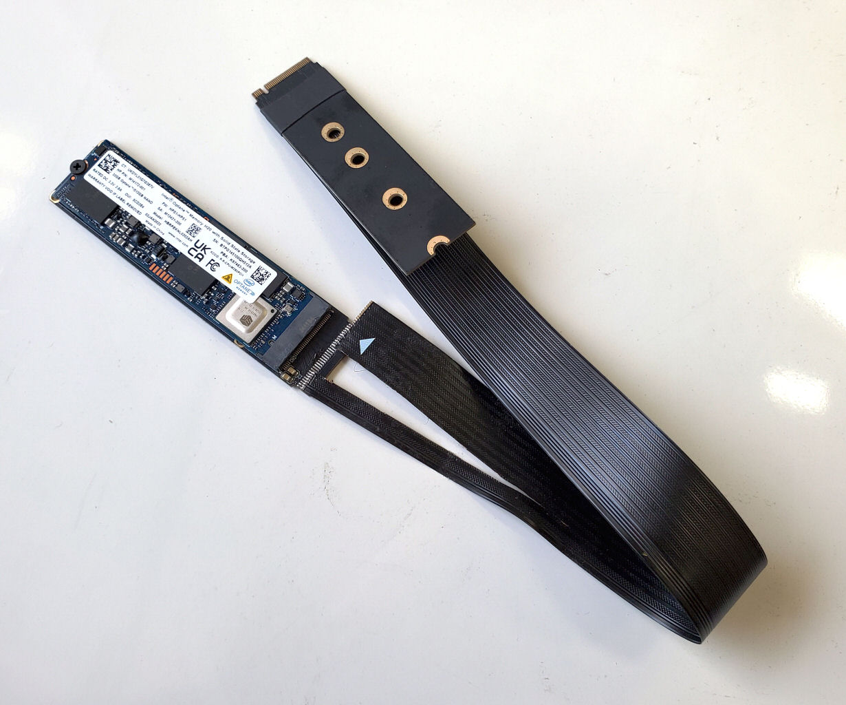 Software tools exist to merge the two data parts back into the full combined volume, but how do you read the Optane memory in the first place? The answer lies in the multiple sets of data signals in the PCI-Express m.2 interface. This standard includes four lanes for data transmission, with each lane consisting of four signals (transmit+, transmit-, receive+, receive-). With typical NVMe SSDs, only one lane is needed to communicate with the drive, while the other lanes merely allow higher throughput. However, hybrid Optane drives allocate some of the lanes to the high-speed Optane/3D XPoint memory part of the drive. That means, with a bit of handiwork, an m.2 ribbon cable extender like the one pictured can be converted into an Optane memory adapter. (Purchase here)
To convert the extender, lane 1 will be rerouted to instead connect to the m.2 socket’s lane 3. First we locate the lanes and trace them to the pins on the ribbon cable, noting the location of the ground pin between RefCLK- and Lane 1 T+ (see diagram below). Then de-solder the ribbon cable from the PCB and use a razor blade or wire cutters to separate the cable between the RefCLK- and Lane 1 T+ wires. (The cable may be pretty stiff, so make sure you split it far enough to be able to flex the cable as much as you need.) Once the cable has been split, solder the first section with the RefCLK pins back to its original location, and reroute and solder the second section so that the Lane 1 and Lane 2 wires are instead connected to Lanes 3 and 4 of the m.2 socket. (This has already been done in the photo below.)
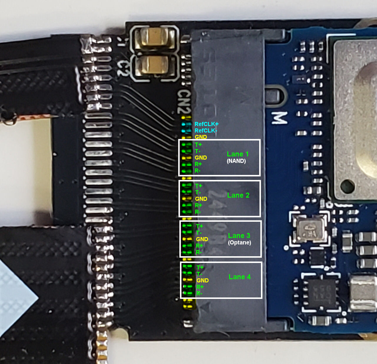
(Click to enlarge)
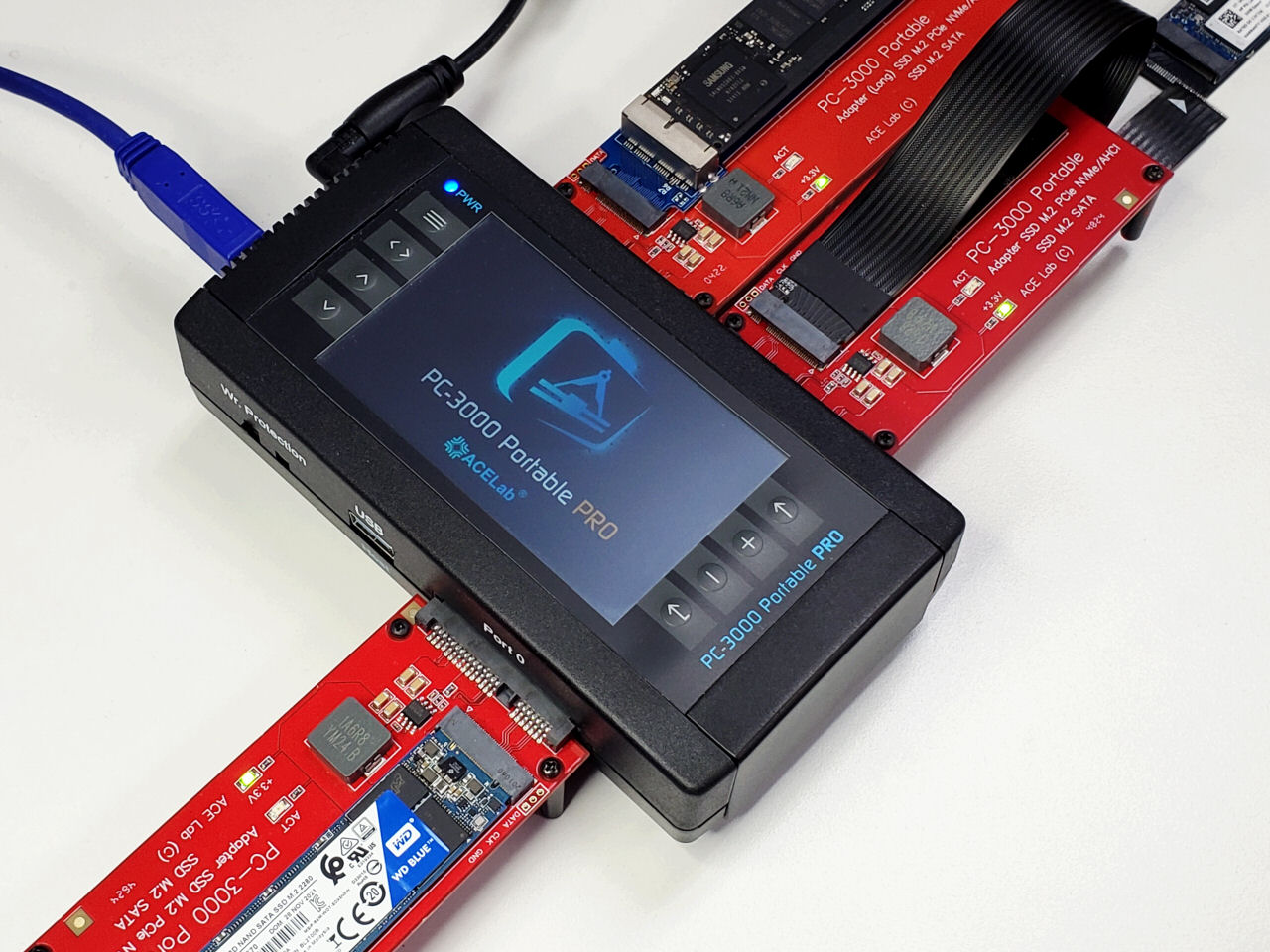 With this modification complete, the Optane memory portion of the drive should now be readily accessible using this adapter. For drives that are in good working condition, the drive can be imaged using a USB adapter or enclosure, but it’s not recommended to attempt to recover drives that are unstable or have bad sectors over a direct USB interface, as that could put your data at risk. Professional tools such as the PC-3000 Portable Pro from Ace Laboratory that we use at Blizzard Data Recovery are recommended to safely recover such drives while minimizing the risk to the data.
And if you’re not confident enough or equipped enough for that, we are here to help with your Intel Optane data recovery!